


 Flexible Thinking: PCB Designers Still Wanted
 Connect the Dots: Five Best Practices for Designing Flex and Rigid-flex PCBs
 Tim’s Takeaways: Human Ingenuity and the Rigid-flex PCB
AT&S Advances PCB, Module and Packaging Technologies
March 1, 2017 | AT&SEstimated reading time: 2 minutes
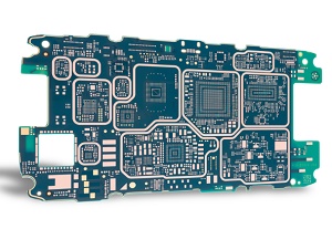
For years, AT&S has worked at the forefront of process and technology development to meet the challenges of continued miniaturization and the demand for better energy efficiency. In this context, the company is involved in various research and development programmes. One current example is the Horizon 2020 EU Research and Innovation programme, in which 11 key European actors are collaborating on the GaNonCMOS project. AT&S is also participating in the Panel-Level Packaging Consortium managed by Fraunhofer IZM.
Optimized energy efficiency with GaN
Over the next four years, the GaNonCMOS project consortium – including AT&S – intends to develop cost‑effective and reliable GaN-based processes, components, modules and integration approaches. In particular, the project aims to exploit the energy-efficiency advantages of GaN (gallium nitride), targeting the production of several demonstrators with GaN power switches and CMOS drivers, as well as new magnetic core materials that will enable switching frequencies up to 200 MHz. Together with optimized embedded PCB technology, the developments should lead to new integrated power components for low-cost, high-reliability systems. Working alongside AT&S on this project are the University of Leuven, Epigan, Fraunhofer, IBM Research, IHP, Tyndall National Institute, PNO Innovation, Recom, NXP Semiconductors and X-FAB Semiconductor.
Advancing miniaturisation with panel-level packaging
The Panel-Level Packaging Consortium has also now been formed. It comprises internationally leading partners such as Intel, ASM Pacific, Hitachi Chemical, AT&S, Evatec, Nanium, Süss MicroTec, Unimicron, Brewer Science, Fujifilm Electronic Materials U.S.A., ShinEtsu, Mitsui Chemicals Tohcello and Semsysco. Together with Fraunhofer IZM as the development hub, the plan is to implement fan-out panel-level packaging (FOPLP), one of the newest packaging trends in microelectronics. FOPLP has a very high miniaturisation potential in both package volume and package density.
During the consortium’s two-year term, known technological elements in wafer-level packaging will be transferred to a large panel format. The technological basis for FOPLP is a reconfigured, moulded panel with embedded components and a thin-film redistribution layer, which together yield an SMD-compatible package. The main advantages of FOPLP are a very thin, substrateless package, low thermal resistance, and good RF characteristics. In addition, passive components such as capacitors, resistors, inductors and antenna structures can be integrated into the redistribution layer. This makes the technology suitable for creating multi-chip packages and System-in-Packages (SiPs).
Based on a panel size of 18″ x 24″ (a PCB manufacturing standard) or even larger sizes, lower packaging costs can be achieved thanks to higher productivity.
Share on:


Suggested Items
Warm Windows and Streamlined Skin Patches – IDTechEx Explores Flexible and Printed Electronics
04/26/2024 | IDTechExFlexible and printed electronics can be integrated into cars and homes to create modern aesthetics that are beneficial and easy to use. From luminous car controls to food labels that communicate the quality of food, the uses of this technology are endless and can upgrade many areas of everyday life.
iNEMI Packaging Tech Topic Series: Role of EDA in Advanced Semiconductor Packaging
04/26/2024 | iNEMIAdvanced semiconductor packaging with heterogenous integration has made on-package integration of multiple chips a crucial part of finding alternatives to transistor scaling. Historically, EDA tools for front-end and back-end design have evolved separately; however, design complexity and the increased number of die-to-die or die-to-substrate interconnections has led to the need for EDA tools that can support integration of overall design planning, implementation, and system analysis in a single cockpit.
Koh Young Showcases Award-winning Inspection Solutions at SMTconnect with SmartRep in Hall 4A.225
04/25/2024 | Koh Young TechnologyKoh Young Technology, the industry leader in True 3D measurement-based inspection solutions, will showcase an array of award-winning inspection and measurement solutions at SMTconnect alongside its sales partner, SmartRep, in booth 4A.225 at NürnbergMesse from June 11-13, 2023. The following offers a glimpse into what Koh Young will present at the tradeshow:
Real Time with… IPC APEX EXPO 2024: Plasmatreat: Innovative Surface Preparation Solutions
04/25/2024 | Real Time with...IPC APEX EXPOIn this interview, Editor Nolan Johnson speaks with Hardev Grewal, CEO and president of Plasmatreat, a developer of atmospheric plasma solutions. Plasmatreat uses clean compressed air and electricity to create plasma, offering environmentally friendly methods for surface preparation. Their technology measures plasma density for process optimization and can remove organic micro-contamination. Nolan and Hardev also discuss REDOX-Tool, a new technology for removing metal oxides.
Nanotechnology Market to Surpass $53.51 Billion by 2031
04/25/2024 | PRNewswireSkyQuest projects that the nanotechnology market will attain a value of USD 53.51 billion by 2031, with a CAGR of 36.4% over the forecast period (2024-2031).