


 Flexible Thinking: PCB Designers Still Wanted
 Connect the Dots: Five Best Practices for Designing Flex and Rigid-flex PCBs
 Tim’s Takeaways: Human Ingenuity and the Rigid-flex PCB
Nano Dimension Strengthening its Leadership Position in 3D Printed Electronics with AME Design Methodology
January 13, 2021 | Nano Dimension Ltd.Estimated reading time: 1 minute
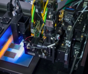
Nano Dimension Ltd., a leading Additively Manufactured Electronics (AME)/PE (Printed Electronics) provider, offers quick solutions and easy access to complex PCBs and 3D printed electronics. Its unique and novel technology allows for rapid prototyping and production of high-performance electronic devices (Hi-PEDs™).
Nano Dimension offers two solutions:
A. DragonFly LDM® 3D-printing system for Hi-PEDs catering to cross-industry needs by enabling in-house printing of free-form, complex, multiple layered boards.
B. A printing service dubbed, NaNoS?, for entities that wish to explore 3D printing of their own designs while gaining access to Nano’s 3D printing and design experts.
“Nano Dimension bridges the gap between PCB and semiconductor integrated circuits,” said Yoav Stern, CEO of Nano Dimension. “A revolution at the click of a button: From CAD to a functional high-performance AME device in hours, solely for the cost of the consumable materials. The DragonFly LDM® should be in everyone’s design workshop for rapid prototyping and testing. AME technology provides the capability to design and create free-form, multilayer complex circuit boards, bringing companies one-step closer to industry 4.0. With NaNoS?, the AME fabrication service becomes the first point of contact and an effective and affordable exploration of AME technology’s capabilities. This is a wake-up call for entities that wish to explore adoption of 3D revolutionary design, manufacturing, and fabrication technology.”
The DragonFly LDM® system enables in-house 3D printing of highly complex, multilayered circuits containing embedded capacitors, antennas, coils, converters, and electro-mechanical components, in just hours.
Nano Dimension’s DragonFly LDM® systems are utilized in cutting edge research institutes, such as CBN-IIT (Italy) and the University of Technology in Sydney (Australia). These institutes continuously expand the design envelope by breaking free from traditional 2D PCB design rules, resulting in miniaturized, performance enhanced 3D AME devices.
With approximately 60 systems sold worldwide, Nano Dimension is also cooperating with customers and partners such as Hensoldt (Germany), L3Harris (USA), and others, to provide insights into how AME technology can drive forward electronics’ design.
Nano Dimension has initiated a webinar-series where scientists and engineers share findings and AME-based solutions in 3D-printed 5G antennas, advanced microwave devices, embedding, micro-electromechanical systems (MEMS) packaging and heterogeneous integration. This knowledge sharing series provides a platform for the free flow of information and an open dialogue between industry experts who are looking for innovative solutions.
Share on:


Suggested Items
Latest Test and Inspection Solutions from GOEPEL electronic at SMTconnect 2024
04/29/2024 | GOEPEL electronicGOEPEL electronic will be demonstrating automated test and inspection equipment at SMTconnect, taking place in Nuremberg from June 11 to 13, 2024.
Arlon Electronic Materials Awarded Requalification to IPC-4101 QPL for All Polyimide Specification Sheets
04/29/2024 | IPCIPC's Validation Services Program has awarded Arlon Electronic Materials Division, an electronics material manufacturing company headquartered in Rancho Cucamonga, Calif., an IPC-4101 Qualified Products Listing (QPL) requalification for the third time.
Warm Windows and Streamlined Skin Patches – IDTechEx Explores Flexible and Printed Electronics
04/26/2024 | IDTechExFlexible and printed electronics can be integrated into cars and homes to create modern aesthetics that are beneficial and easy to use. From luminous car controls to food labels that communicate the quality of food, the uses of this technology are endless and can upgrade many areas of everyday life.
Book Excerpt: The Printed Circuit Assembler’s Guide to... Factory Analytics
04/24/2024 | I-Connect007 Editorial TeamIn our fast-changing, deeply competitive, and margin-tight industry, factory analytics can be the key to unlocking untapped improvements to guarantee a thriving business. On top of that, electronics manufacturers are facing a tremendous burden to do more with less. If you don't already have a copy of this book, what follows is an excerpt from the introduction chapter of 'The Printed Circuit Assembler’s Guide to... Factory Analytics: Unlocking Efficiency Through Data Insights' to whet your appetite.
Listen Up! The Intricacies of PCB Drilling Detailed in New Podcast Episode
04/25/2024 | I-Connect007In episode 5 of the podcast series, On the Line With: Designing for Reality, Nolan Johnson and Matt Stevenson continue down the manufacturing process, this time focusing on the post-lamination drilling process for PCBs. Matt and Nolan delve into the intricacies of the PCB drilling process, highlighting the importance of hole quality, drill parameters, and design optimization to ensure smooth manufacturing. The conversation covers topics such as drill bit sizes, aspect ratios, vias, challenges in drilling, and ways to enhance efficiency in the drilling department.