


 Punching Out: Breaking Out of the Valuation Box
 Happy’s Tech Talk #28: The Power Mesh Architecture for PCBs
 It’s Only Common Sense: Would You Join Your Own Company?
Aven's New Wide-View UV Magnifier with White & Ultraviolet LEDs
January 31, 2023 | AvenEstimated reading time: Less than a minute
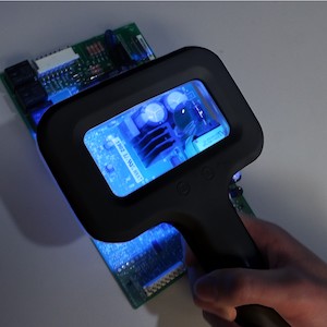
Aven, a full-service technology provider, is pleased to introduce its Wide-View Magnifier [2.25x | 4x] with Ultraviolet and White LEDs. Convenient and easy-to-use, Aven’s Wide-View UV Magnifier features a 3.6 x 1.7” rectangular glass, providing a wide viewing area. The 5-diopter lens offers up to 2.25X magnification, and the 1” diameter spot lens increases the magnification to 4X.
Operating at 365 ?m, the UV LEDs are exceptionally bright when illuminating objects that fluoresce, such as paper, ink, circuit boards, money, etc. The 26 UV LEDs shine brightly to reveal fluoresced details that standard lights cannot show.
The Wide-View Magnifier is ideal for dermatology, trauma, schools, ophthalmology, forensic science, hospitality/food industry, agriculture, and industrial inspection for detecting defects. The ESD-safe design helps to dissipate static electric charges, protecting sensitive components below from unintentional damage.
As a result of years of comprehensive research and development, Aven has expanded its expertise in the realm of design and customized configuration of advanced video inspection systems. The company’s solution-based experts possess the ability to recommend and create complete optical systems according to customers’ needs and budgets.
Share on:


Suggested Items
EMA Webinar: Next Generation MCAD/ECAD for SOLIDWORKS
05/09/2024 | EMA Design AutomationLearn how the MCAD and ECAD experts at Hawk Ridge and EMA can help you solve your MCAD/ECAD integration challenges with this unique collaboration environment.
Sondrel Awarded New Video Processor ASIC Design and Supply Contract
05/09/2024 | SondrelSondrel, a leading provider of ultra-complex custom chips for leading global technology brands, is pleased to announce that it has won a major ASIC design and supply contract for a next generation, video processing chip.
Connect the Dots: Designing for Reality—The Pre-Manufacturing Process
05/08/2024 | Matt Stevenson -- Column: Connect the DotsI have been working with Nolan Johnson on a podcast series about designing PCBs for the reality of manufacturing. By sharing lessons learned over a long career in the PCB industry, we hope to shorten learning curves and help designers produce better boards with less hassle and rework. Episode 2 deals with the electronic pre-manufacturing process. Moving from CAD (computer-aided design) to CAM (computer-aided manufacturing) is a key step in PCB manufacturing. CAM turns digital designs into instructions that machines can use to actually build the PCB.
Indium Corporation to Showcase HIA Materials at ECTC
05/07/2024 | Indium CorporationAs an industry leader in innovative materials solutions for semiconductor packaging and assembly, Indium Corporation® will feature its advanced products designed to meet the evolving challenges of heterogeneous integration and assembly (HIA) and fine-pitch system-in-package (SiP) applications at the 74th Electronic Components and Technology Conference (ECTC), May 28‒31, in Denver, Colorado.
Siemens Delivers New Solido IP Validation Suite
05/07/2024 | SiemensSiemens Digital Industries Software introduced Solido™ IP Validation Suite software, a comprehensive, automated signoff solution for quality assurance across all design intellectual property (IP) types, including standard cells, memories and IP blocks.