


 The Right Approach: I Hear the Train A Comin'
 It’s Only Common Sense: OCCAM—the Time Is Now
 Marcy's Musings: The Growing Industry
Inkjet Printable and Biocompatible Layered Electronics
March 29, 2017 | Graphene FlagshipEstimated reading time: 4 minutes
Printed electronics can lead to both low-cost and flexible devices. Flexible electronics is of particular interest for wearable systems, such as health and fitness trackers, while the relative low-costs of printing are attractive for functional packaging for consumer products. Graphene and related layered materials (GRMs) are ideal for printed electronics because they can be readily solution processed into inks that have excellent electronic properties.
In a step toward rapid and low-cost prototyping of electronic devices, researchers from the Graphene Flagship have demonstrated fully inkjet printed programmable memory devices, using biocompatible water-based inks.
Now, biocompatible, water-based inks containing GRMs have been developed as building blocks for inkjet printable electronic devices. Importantly, the inks can be used to successfully inkjet print electronic devices based on combinations of different layered materials. The research, published in Nature Nanotechnology, was performed in a collaboration between researchers at the University of Manchester, UK and the University of Pisa, Italy.
Inkjet printing
The GRM inks containing conductive graphene, the insulator hexagonal boron nitride (hBN) and semiconductor transition metal dichalcogenides (TMDs), such as MoS2 and WS2, provide the full range of electronic properties needed to print complex electronics, including photodetectors. The inks can be printed onto flexible and stiff substrates, such as paper, glass and plastic, and the inks’ biocompatibility also suggests possibilities for printing biomedical devices such as sensor implants.
Inkjet printing is attractive as a fast and accessible route to printed electronics, because of simple switching of design and materials. The devices were produced using a material inkjet printer available in the market, demonstrating the suitability of this technique as a platform for rapid prototyping (similar to 3D printing), while paving the way towards print-on-demand electronics.
Gianluca Fiori, a researcher at the department of Information Engineering at the University of Pisa, Italy, said “We are now entering a new scenario in the field of electronics, where electronic systems can be printed on demand and on flexible substrates as paper. GRMs based inks could indeed represent an enabling technology for the fast-growing market of flexible and portable electronics.”
Printed memory
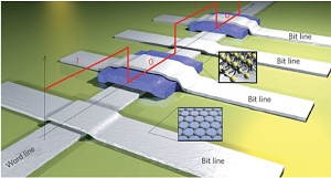
The inks were used to print photodetectors and the first inkjet printable read-only memory, in the form of an array of bit-strips using graphene and WS2 inks. Such readable memory could be ideal for identification numbers in radio-frequency identification (RFID) tags, and could be developed further into more complex memory systems when integrated with other printed devices such as diodes and transistors.
Heterostructures, made of stacked layers of different materials, are important for compact integration of functional circuits. Typically, with inkjet printing it is very difficult to obtain good interfaces, meaning the printed devices do not operate reliably. For these new inks, the researchers optimised the ink formula specifically for inkjet printing, adding xantham gum as a binder to prevent the printed interfaces merging together.
The research was led by Cinzia Casiraghi, a researcher in the School of Chemistry at the University of Manchester, UK. She explained that the printable heterostructures are “the first step towards the realization of low-cost and flexible devices.” Outlining the challenges that this research overcomes, she said “Currently, heterostructures are formed by two or three layers and only very few examples of more complex heterostructures have been demonstrated, using non-scalable techniques. We are now in the position to fabricate devices of arbitrary geometry on a flexible substrate. For example, we can produce arrays of heterostructures, where every junction can be designed ad hoc to store or sense a particular type of information.”
A printed future
One important area where these printed circuits could find application is in smart packaging. The Internet of Things is enabling connectivity in an unprecedented range of applications, and smart packaging could be ideal for managing inventories and monitoring spoilage in food, drinks and pharmaceuticals; applications for which the ink’s biocompatibility is essential. “We are also very excited about the possibility of implementing logic circuits made of these materials – indeed, we are further developing these type of devices,” added Casiraghi.
Coşkun Kocabaş, a researcher at Bilkent University, Turkey, is Deputy Leader of the Partnering Division of the Graphene Flagship, where Casiraghi's ERC project NOC2D is affiliated. “This method provides the advantage of heterogeneous integration of conducting, semiconducting and dielectric layered materials. This capability will enable new directions in electronics aiming to generate very large scale and low cost circuits,” he said. “Another exciting next step would be integration of this method with 3D printing techniques which could enable printed circuits with exotic topologies.”
Andrea Ferrari, Science and Technology Officer and Chair of the Management Panel of the Graphene Flagship added "Printed and flexible electronics has been at the core of the Graphene Flagship since its beginning and is certainly one of the key areas where graphene and related materials can find near-term applications. This work is an important step forward, and demonstrates the successful collaboration of between the Flagship Core 1 Partners and the newly formed partnering division, further strengthening the Flagship as the European hub for innovation in graphene and related materials."
Share on:


Suggested Items
Warm Windows and Streamlined Skin Patches – IDTechEx Explores Flexible and Printed Electronics
04/26/2024 | IDTechExFlexible and printed electronics can be integrated into cars and homes to create modern aesthetics that are beneficial and easy to use. From luminous car controls to food labels that communicate the quality of food, the uses of this technology are endless and can upgrade many areas of everyday life.
Book Excerpt: The Printed Circuit Assembler’s Guide to... Factory Analytics
04/24/2024 | I-Connect007 Editorial TeamIn our fast-changing, deeply competitive, and margin-tight industry, factory analytics can be the key to unlocking untapped improvements to guarantee a thriving business. On top of that, electronics manufacturers are facing a tremendous burden to do more with less. If you don't already have a copy of this book, what follows is an excerpt from the introduction chapter of 'The Printed Circuit Assembler’s Guide to... Factory Analytics: Unlocking Efficiency Through Data Insights' to whet your appetite.
Listen Up! The Intricacies of PCB Drilling Detailed in New Podcast Episode
04/25/2024 | I-Connect007In episode 5 of the podcast series, On the Line With: Designing for Reality, Nolan Johnson and Matt Stevenson continue down the manufacturing process, this time focusing on the post-lamination drilling process for PCBs. Matt and Nolan delve into the intricacies of the PCB drilling process, highlighting the importance of hole quality, drill parameters, and design optimization to ensure smooth manufacturing. The conversation covers topics such as drill bit sizes, aspect ratios, vias, challenges in drilling, and ways to enhance efficiency in the drilling department.
Elevating PCB Design Engineering With IPC Programs
04/24/2024 | Cory Blaylock, IPCIn a monumental stride for the electronics manufacturing industry, IPC has successfully championed the recognition of the PCB Design Engineer as an official occupation by the U.S. Department of Labor (DOL). This pivotal achievement not only underscores the critical role of PCB design engineers within the technology landscape, but also marks the beginning of a transformative journey toward nurturing a robust, skilled workforce ready to propel our industry into the future.
Winner of The Science Show Rakett 69 Receives Incap Scholarship
04/24/2024 | IncapThe winner of the Rakett 69 science show, Andri Türkson, who stood out as an electronics enthusiast, received a scholarship from Incap Estonia, along with an internship opportunity in Saaremaa.