


 Flexible Thinking: PCB Designers Still Wanted
 Connect the Dots: Five Best Practices for Designing Flex and Rigid-flex PCBs
 Tim’s Takeaways: Human Ingenuity and the Rigid-flex PCB
Biodegradable Electronics
October 13, 2017 | Fraunhofer FEPEstimated reading time: 1 minute
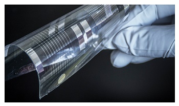
Under the direction of the Fraunhofer Institute for Organic Electronics, Electron Beam and Plasma Technology FEP, an in-house Fraunhofer project for development of biodegradable electronics was begun last year. The Fraunhofer Institute for Electronic Nano Systems ENAS, the Fraunhofer Institute for Biomedical Engineering IBMT, the Fraunhofer Institute for Silicate Research ISC, and the Fraunhofer Resource Recycling and Strategy Project Group IWKS are working together on the project.
Electronic components that are completely broken down in a biological environment after a pre-defined operating life open up novel applications as well as ways for reducing their ecological footprint.
One enabling technology for such components is the manufacture of biodegradable conductive traces on biodegradable substrates using vacuum technologies. This technology was developed by Fraunhofer FEP.
A novel application area for these innovative electronic components for example is in the field of active medical implants that after expiration of their operating life are resorbed by tissue, thereby sparing the patient a second surgical intervention.
The Fraunhofer Gesellschaft e. V. is now funding the "bioElektron - Biodegradable Electronics for Active Implants" project through its in-house program (funding No. MAVO B31 301). The goal of the project is the development of essential components for biodegradable electronic parts that can be employed for example in an implant.
This includes in particular:
- biodegradable conductor structures
- biodegradable electrodes for collecting electrical signals or delivering electrical stimulation
- biodegradable thin-film transistors and circuitry
- biodegradable barrier coatings as moisture and gas barriers, and electrical insulation layers
These elements will be monolithically integrated into a flexible thin-film device.
Conductor structures and organic thin-film transistors are being developed at Fraunhofer FEP using vacuum technology. Deposition of magnesium via thermal evaporation under high vacuum conditions is being used as an enabling technology for this purpose. Magnesium is known for being a biodegradable and biologically compatible metal that is already employed in clinical environments as an absorbable implant material. The challenge consists of depositing this metal upon biodegradable polymer films that magnesium does not adhere sufficiently to under normal process control. By suitably pre-treating the substrates using a combination of drying, plasma treatment, and utilization of seed layers, finely structured high-quality conductor structures were able to be produced.
Share on:


Suggested Items
IDTechEx Explores the Role of 3D Cu-Cu Hybrid Bonding in Powering Future HPC and AI Products
04/18/2024 | PRNewswireSemiconductor packaging has evolved from traditional 1D PCB levels to cutting-edge 3D hybrid bonding at the wafer level, achieving interconnecting pitches as small as single micrometers and over 1000 GB/s bandwidth. Key parameters, including Power, Performance, Area, and Cost, are crucial considerations
Intel Brings AI-Platform Innovation to Life at the Olympic Games
04/18/2024 | BUSINESS WIREIntel announced its plans for the Olympic and Paralympic Games Paris 2024. Bringing AI Everywhere, Intel will implement artificial intelligence technology powered by Intel processors on the world’s biggest stage.
Adura Solutions Exhibits at Del Mar 2024
04/18/2024 | Adura SolutionsSumit Tomar, CEO of Adura Solutions, has announced that his company will be exhibiting at this year's Del Mar Electronics and Manufacturing Show to be held at the Del Mar Fairgrounds, San Diego, California, April 24-25.
Australian Flow Batteries and The SCHMID Group Announce Groundbreaking Memorandum of Understanding
04/17/2024 | SCHMID GroupAustralian Flow Batteries Pty Ltd (AFB), a leader in innovative energy solutions and economical, safe, and reliable power storage, and SCHMID Energy Systems GmbH a company of the German SCHMID Group, a global technology leader with a rich history in delivering innovative solutions across multiple industries including Electronics, Renewables, and Energy Storage sectors, are thrilled to announce the signing of a Memorandum of Understanding (MoU)
Ansys Joins BAE Systems’ Mission Advantage Program to Advance Digital Engineering Across US Department of Defense
04/16/2024 | ANSYSAnsys announced it is working with BAE Systems, Inc., to accelerate the adoption of digital engineering and MBSE across the Department of Defense (DoD).