


 Marcy's Musings: The Growing Industry
 It’s Only Common Sense: Here’s What To Do After IPC APEX EXPO 2024
 Dan’s Biz Bookshelf: Seeing the How
Atotech Launches New Horizontal Bonding Enhancement Solution for HF Applications
April 26, 2018 | AtotechEstimated reading time: 2 minutes
BondFilm HF is Atotech’s new process for the treatment of inner layer cores. It leads to highest bonding performance in the manufacture of multilayer & HDI printed circuit boards. This innovative new process maintains the excellent performance first developed in the BondFilm product range whilst offering the lowest possible signal loss as required in high frequency applications.
Circuit design is already planning towards the low signal loss requirements of the next generation of network technology, the so called 5G. To meet these signal integrity demands the ideal would be to use a non-etching adhesion promotor system. However, whilst such systems are available in the market, they are not yet widely established. BondFilm HF bridges the gap with significantly reduced surface roughening which helps meet the signal integrity requirements whilst maintaining excellent bond strength and functional performance.
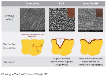
BondFilm HF
The latest development in Atotech’s BondFilm product range is BondFilm HF. Copper panels treated with BondFilm HF have the typical uniform, brown organo-metallic coating long associated with the BondFilm® process. This coating retains the excellent enhanced bonding between the inner layer and prepregs used in multilayer manufacture but with one significant difference: only minimal roughening is needed.
In previous versions of the BondFilm process development targets have been to maximize the surface roughening to give the best possible multilayer bond strength; here, the target was to provide this functional performance without compromise but with a minimal roughening of the copper traces. By producing this low roughening of the copper surface a significant reduction in signal loss in the „skin“ of the copper traces is achieved. This makes BondFilm HF more suited to high frequency applications where signal integrity is paramount.
Production trials using BondFilm HF focused on the functional properties of the multilayer boards together with electrical signal loss measurements. Data shows that panels manufactured with BondFilm HF fulfill all reliability tests considered, such as thermal stress tests and performance multiple iR reflow cycles. At the same time they significantly outperform panels made with conventional treatment processes in terms of reduced signal loss.
BondFilm HF is a simple drop in replacement for existing BondFilm process users. Its short process sequence is also compatible with most existing oxide alternative lines.
The process is already installed in a leading Chinese manufacturer and shows excellent results with first customer evaluations. Its key benefits in terms of significantly reduced signal loss gives this new process a considerable advantage for all high frequency applications.
About Atotech
Atotech is one of the world’s leading manufacturers of specialty chemicals and equipment for the printed circuit board, IC-substrate and semiconductor industries, as well as for the decorative and functional surface finishing industries. Atotech has annual sales of USD1.2 billion (2017). The company is fully committed to sustainability – we develop technologies to minimize waste and to reduce environmental impact. Atotech has its headquarters in Berlin, Germany, and employs about 4,000 people in over 40 countries. About a quarter of all staff works in one of the four locations in Germany: Berlin, Feucht, Neuruppin, and Trebur. For more information, click here.
Share on:


Suggested Items
Insulectro’s 'Storekeepers' Extend Their Welcome to Technology Village at IPC APEX EXPO
04/03/2024 | InsulectroInsulectro, the largest distributor of materials for use in the manufacture of PCBs and printed electronics, welcomes attendees to its TECHNOLOGY VILLAGE during this year’s IPC APEX EXPO at the Anaheim Convention Center, April 9-11, 2024.
ENNOVI Introduces a New Flexible Circuit Production Process for Low Voltage Connectivity in EV Battery Cell Contacting Systems
04/03/2024 | PRNewswireENNOVI, a mobility electrification solutions partner, introduces a more advanced and sustainable way of producing flexible circuits for low voltage signals in electric vehicle (EV) battery cell contacting systems.
Heavy Copper PCBs: Bridging the Gap Between Design and Fabrication, Part 1
04/01/2024 | Yash Sutariya, Saturn Electronics ServicesThey call me Sparky. This is due to my talent for getting shocked by a variety of voltages and because I cannot seem to keep my hands out of power control cabinets. While I do not have the time to throw the knife switch to the off position, that doesn’t stop me from sticking screwdrivers into the fuse boxes. In all honesty, I’m lucky to be alive. Fortunately, I also have a talent for building high-voltage heavy copper circuit boards. Since this is where I spend most of my time, I can guide you through some potential design for manufacturability (DFM) hazards you may encounter with heavy copper design.
Trouble in Your Tank: Supporting IC Substrates and Advanced Packaging, Part 5
03/19/2024 | Michael Carano -- Column: Trouble in Your TankDirect metallization systems based on conductive graphite or carbon dispersion are quickly gaining acceptance worldwide. Indeed, the environmental and productivity gains one can achieve with these processes are outstanding. In today’s highly competitive and litigious environment, direct metallization reduces costs associated with compliance, waste treatment, and legal issues related to chemical exposure. What makes these processes leaders in the direct metallization space?
AT&S Shines with Purest Copper on World Recycling Day
03/18/2024 | AT&SThe Styrian microelectronics specialist AT&S is taking World Recycling Day as an opportunity to review the progress that has been made in recent months at its sites around the world in terms of the efficient use of resources: