


 Marcy's Musings: The Growing Industry
 It’s Only Common Sense: Here’s What To Do After IPC APEX EXPO 2024
 Dan’s Biz Bookshelf: Seeing the How
AT&S Offers a Look into the Future of Connection Technology
May 2, 2018 | AT&SEstimated reading time: 4 minutes
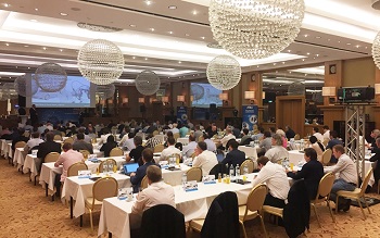
In Velden (Austria), AT&S presented innovative technologies and trends in connection solutions at the 14th AT&S Technology Forum. Numerous interested customers were able to find out about the latest developments in the electronics and printed circuit board industry for areas such as mobile devices, automotive, industrial, communications and medical technology and to exchange views with the AT&S experts. The broad-based lectures focused on global trends such as 5G mobile communications, autonomous driving or increasingly networked systems and the associated requirements for connection technology.
The main challenges posed include the integration of far-reaching functionalities, advancing miniaturization, higher power densities with demanding thermal requirements, high data rates with high signal speeds and short latencies as well as optimized production processes and materials. Miniaturization can only be achieved by increasing the packing density of electronic components, which sees PCB and semiconductor technologies converging. Among other things, AT&S offers a combination of existing and new technologies (AT&S Toolbox), which are designed to work perfectly with each other.
To date, there has been a gap between wafer/chip technologies (fan-out wafer level packaging, flip-chip BGA, interposer-based components) on the one hand, and the PCB/substrate infrastructure on the other for an optimized, miniaturized packaging design. The structure widths (track/distance) on the chip side are approximately between 2/2 and 8/8 mm and on the PCB side currently around 30/30 mm. For further miniaturization it is important to close this gap. To achieve this, AT&S is currently using mSAP (modified semi-additive process) – in other words, printed circuit board-like substrates, which permit highly miniaturized and precise structures. Against this backdrop, the roadmap envisages combining PCB technologies (HDI), substrates, embedded technology and possibly active thermal management and shielding to ultimately realize AiOP (all-in-one package) solutions.
“Given the current megatrends such as 5G, networked systems, autonomous driving and M2M communication with ever higher data rates and volumes as well as high power densities, the demands on connection technology are also increasing,” said Walter Moser, CSO of the Automotive, Industrial and Medical business unit at AT&S and moderator of the technology forum. “As the technology forum has clearly demonstrated, AT&S has worked closely with its customers to deliver a host of innovative solutions so as to continue to offer technology-leading and cost-effective products also in future.”
The introduction of the new generation of mobile communications (5G with frequency bands up to 6 GHz and significantly higher), but also automated/autonomous driving supported by powerful radar systems (77 GHz) are clear examples of the increasing demands on data rates and signal integrity. For connection technology manufacturers, this means, for example, reducing signal losses and disturbances by optimizing the dielectric material, the material interfaces and also the copper roughness. In the latter case, for example, it is necessary to overcome the dilemma that, although less rough copper offers advantages for HF applications, a somewhat higher roughness improves the adhesion during printed circuit board pressing. The geometry (profile) of the tracks also affects signal delays at higher frequencies. In addition, AT&S is also investigating the influence of various metals on the skin effect in the GHz range and, accordingly, is developing new surface materials.
At the forum, high-frequency requirements were also discussed intensively in a number of lectures. Modern simulation tools such as those used by AT&S together with its partners facilitate simulation early in the design phase, for example. Several lectures discussed the requirements and solutions in terms of system integration (embedded technologies, hybrid boards, embedding cavities, etc.), the structuring for further miniaturization (thinner printed circuit boards, coplanarity, finer tracks and vias, reduction of the coefficient of thermal expansion (CTE), conductor profile, etc.) and the thermal management with current solutions (heat spread, thermal vias and inlays) and future technologies (heat pipes, embedding of cooling elements, etc.).
The conference also covered other current topics relating to connection technology, such as the embedded power of powerful chips (MOSFETs, etc.) in the printed circuit board, the failure analysis of printed circuit boards, and the investigation of material reliability in solder joint connections. For the customers, however, less technological aspects and lectures were also interesting, such as cost-efficient design with HDI printed circuit boards as well as the targeted use of the IPC2 and IPC3 classes – both depending on the respective application.
At AT&S, we are perfectly positioned for the future requirements. More than 400 research and development (R&D) staff are currently employed worldwide, and the company re-invests almost 8% of its revenue in R&D. One outcome of this is the close cooperation with international partners and more than 230 registered patents. In addition to research and development focusing on Austria, state-of-the-art production facilities are available in Austria, China, Korea and India. More recently, AT&S has announced an investment of approximately €40 million for technology expansion and capacity building for high-frequency printed circuit boards at its existing sites in Nanjangud, India and Fehring, Austria. This is designed in particular to support the growth potential in the field of autonomous driving.
Share on:


Suggested Items
AIM to Highlight NC259FPA Ultrafine No Clean Solder Paste at SMTA Wisconsin Expo & Tech Forum
04/18/2024 | AIMAIM Solder, a leading global manufacturer of solder assembly materials for the electronics industry, is pleased to announce its participation in the upcoming SMTA Wisconsin Expo & Tech Forum taking place on May 7 at the Four Points by Sheraton | Milwaukee Airport, in Milwaukee, Wisconsin.
Hentec/RPS Publishes an Essential Guide to Selective Soldering Processing Tech Paper
04/17/2024 | Hentec Industries/RPS AutomationHentec Industries/RPS Automation, a leading manufacturer of selective soldering, lead tinning and solderability test equipment, announces that it has published a technical paper describing the critical process parameters that need to be optimized to ensure optimal results and guarantee the utmost in end-product quality.
Empowering Electronics Assembly: Introducing ALPHA Innolot MXE Alloy
04/16/2024 | MacDermid Alpha Electronics SolutionsIn the rapidly evolving electronics industry, where innovation drives progress, MacDermid Alpha Electronics Solutions is committed to setting a new standard. Today, we are pleased to introduce ALPHA Innolot MXE, a revolutionary alloy meticulously engineered to address the critical needs of enhanced reliability and performance in modern electronic assemblies.
New Book on Low-temperature Soldering Now Available
04/17/2024 | I-Connect007I-Connect007 is pleased to announce that The Printed Circuit Assembler’s Guide to… Low-temperature Soldering, Vol. 2, by subject matter experts at MacDermid Alpha Electronics Solutions, is now available for download.
Inkjet Solder Mask ‘Has Arrived’
04/10/2024 | Pete Starkey, I-Connect007I was delighted to be invited to attend an interactive webinar entitled “Solder Mask Coating Made Easy with Additive Manufacturing,” hosted by SUSS MicroTec Netherlands in Eindhoven. The webinar was introduced and moderated by André Bodegom, managing director at Adeon Technologies, and the speakers were Mariana Van Dam, senior product manager PCB imaging solutions at AGFA in Belgium; Ashley Steers, sales manager at Electra Polymers in the UK; and Dr. Luca Gautero, product manager at SUSS MicroTec Netherlands.