


 Flexible Thinking: PCB Designers Still Wanted
 Connect the Dots: Five Best Practices for Designing Flex and Rigid-flex PCBs
 Tim’s Takeaways: Human Ingenuity and the Rigid-flex PCB
Quantum Interferometry Demonstrated in Silicon at More Practical Temperatures
August 6, 2019 | RIKENEstimated reading time: 2 minutes
Using a silicon-based transistor similar to those found in everyday electronics, RIKEN researchers have produced a functional quantum ‘qubit’—the quantum equivalent of bits used in conventional computers—that operates above the extremely low temperatures typically needed to observe quantum interference effects.
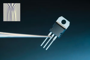
Image Caption: Figure 1: By fabricating a simple three-terminal device that is similar to a general transistor using standard microfabrication techniques, RIKEN researchers could observe quantum interference effects of a single qubit while continuously varying the energy level of the qubit (inset).
The study breaks open the exploration of quantum interference to enable research using standard materials and techniques at more accessible temperatures.
Many highly sensitive measurement techniques are based on monitoring the interference of waves. The most well-known example is the detection of extremely weak gravitational waves generated by colliding neutron stars and black holes using the interference between two laser beams that are several kilometers long. Many scientists are working on extending this technique to the wave functions of quantum objects since this would permit much more sensitive sensing than is possible using classical waves.
A promising system for achieving such quantum interferometry is silicon because researchers can draw on the many decades of research and development that have gone into conventional silicon-based electronics and integrated circuits. In particular, spin qubits in silicon could be used for quantum interferometry, but semiconductor qubits typically need temperatures very close to absolute zero, which necessitates using bulky and expensive cryogenic equipment.
Now, Keiji Ono of the RIKEN Advanced Device Laboratory and his co-workers have raised the operating temperature of qubits in silicon to 1.6 kelvin. “This is in the ‘high temperature’ range, which might sound strange, but compared with the 0.1 kelvin temperatures usually required for semiconductor qubits, these high temperatures can be produced in a less expensive, smaller facility and in a short time,” comments Ono. “This is a major achievement and will reduce the hurdles for any research group trying to enter this area of research and development.”
The researchers fabricated a simple three-terminal device similar to a general transistor using standard microfabrication techniques, and were able to observe the quantum interference effects of the single qubit while continuously varying the energy level of the qubit (inset of Fig. 1).
“I wanted to use a silicon device as a universal basis for exploring ubiquitous, material-independent quantum effects,” explains Ono. “Furthermore, our device is not just a laboratory device made using silicon material, but a practical device that actually forms part of a large-scale integrated circuit.”
The results that the team obtained using the device agreed well with theory. “Our single qubit calculates the weighted average of two input variables using quantum interference,” says Ono. “We achieved almost perfect agreement between the experiments and calculations, confirming the ubiquitous nature of the observed quantum interference effect.”
Share on:


Suggested Items
Nanotechnology Market to Surpass $53.51 Billion by 2031
04/25/2024 | PRNewswireSkyQuest projects that the nanotechnology market will attain a value of USD 53.51 billion by 2031, with a CAGR of 36.4% over the forecast period (2024-2031).
DOCOMO, NTT, NEC and Fujitsu Develop Top-level Sub-terahertz 6G Device
04/12/2024 | JCN NewswireNTT DOCOMO, INC., NTT Corporation, NEC Corporation and Fujitsu Limited jointly announced today the development of a top-level (1) wireless device capable of ultra-high-speed 100 Gbps transmissions in the 100 GHz and 300 GHz sub-terahertz bands.
Keysight Becomes Validated Test Tool Provider for FiRa 2.0 Technical and Test Specifications
04/05/2024 | Keysight Technologies, Inc.Keysight Technologies, Inc. has had a test tool validated for the FiRa 2.0 Certification release, covering physical layer (PHY) conformance testing. The latest FiRa PHY Technical and Test Specifications introduce enhancements to the performance and interoperability test requirements for ultra-wideband (UWB) device conformance tests.
Scientists Propose a New Way to Search for Dark Matter
04/02/2024 | SLAC National Accelerator LaboratoryEver since its discovery, dark matter has remained invisible to scientists, despite the launch of multiple ultra-sensitive particle detector experiments around the world over several decades.
INSPECTIS Offers Slider Plate Stand for Optical Inspection
04/01/2024 | INSPECTISINSPECTIS introduces a new specialized slider stand capability for repetitive optical inspection tasks, for example, for the production of special devices such as stents.