


 Flexible Thinking: PCB Designers Still Wanted
 Connect the Dots: Five Best Practices for Designing Flex and Rigid-flex PCBs
 Tim’s Takeaways: Human Ingenuity and the Rigid-flex PCB
Stanford Researchers Develop New Manufacturing Technique for Flexible Electronics
June 30, 2021 | Andrew Myers, Stanford UniversityEstimated reading time: 4 minutes
Ultrathin, flexible computer circuits have been an engineering goal for years, but technical hurdles have prevented the degree of miniaturization necessary to achieve high performance. Now, researchers at Stanford University have invented a manufacturing technique that yields flexible, atomically thin transistors less than 100 nanometers in length – several times smaller than previously possible. The technique is detailed in a paper published June 17 in Nature Electronics.
With the advance, said the researchers, so-called “flextronics” move closer to reality. Flexible electronics promise bendable, shapeable, yet energy-efficient computer circuits that can be worn on or implanted in the human body to perform myriad health-related tasks. What’s more, the coming “internet of things,” in which almost every device in our lives is integrated and interconnected with flexible electronics, should similarly benefit from flextronics.
Technical difficulties
Among suitable materials for flexible electronics, two-dimensional (2D) semiconductors have shown promise because of their excellent mechanical and electrical properties, even at the nanoscale, making them better candidates than conventional silicon or organic materials.
The engineering challenge to date has been that forming these almost impossibly thin devices requires a process that is far too heat-intensive for the flexible plastic substrates. These flexible materials would simply melt and decompose in the production process.
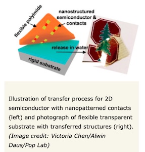
The solution, according to Eric Pop, a professor of electrical engineering at Stanford, and Alwin Daus, a postdoctoral scholar in Pop’s lab, who developed the technique, is to do it in steps, starting with a base substrate that is anything but flexible.
Atop a solid slab of silicon coated with glass, Pop and Daus form an atomically thin film of the 2D semiconductor molybdenum disulfide (MoS2) overlaid with small nano-patterned gold electrodes. Because this step is performed on the conventional silicon substrate, the nanoscale transistor dimensions can be patterned with existing advanced patterning techniques, achieving a resolution otherwise impossible on flexible plastic substrates.
The layering technique, known as chemical vapor deposition (CVD), grows a film of MoS2 one layer of atoms at a time. The resulting film is just three atoms thick, but requires temperatures reaching 850 C (over 1500 F) to work. By comparison, the flexible substrate – made of polyimide, a thin plastic – would long ago have lost its shape somewhere around 360 C (680 F), and completely decomposed at higher temperatures.
By first patterning and forming these critical parts on rigid silicon and allowing them to cool, the Stanford researchers can apply the flexible material without damage. With a simple bath in deionized water, the entire device stack peels back, now fully transferred to the flexible polyimide.
After few additional fabrication steps, the results are flexible transistors capable of several times higher performance than any produced before with atomically thin semiconductors. The researchers said that while entire circuits could be built and then transferred to the flexible material, certain complications with subsequent layers make these additional steps easier after transfer.
“In the end, the entire structure is just 5 microns thick, including the flexible polyimide,” said Pop, who is senior author of the paper. “That’s about ten times thinner than a human hair.”
While the technical achievement in producing nanoscale transistors on a flexible material is notable in its own right, the researchers also described their devices as “high performance,” which in this context means that they are able to handle high electrical currents while operating at low voltage, as required for low power consumption.
“This downscaling has several benefits,” said Daus, who is first author of the paper. “You can fit more transistors in a given footprint, of course, but you can also have higher currents at lower voltage – high speed with less power consumption.”
Meanwhile, the gold metal contacts dissipate and spread the heat generated by the transistors while in use – heat which might otherwise jeopardize the flexible polyimide.
Promising future
With a prototype and patent application complete, Daus and Pop have moved on to their next challenges of refining the devices. They have built similar transistors using two other atomically thin semiconductors (MoSe2 and WSe2) to demonstrate the broad applicability of the technique.
Meanwhile, Daus said that he is looking into integrating radio circuitry with the devices, which will allow future variations to communicate wirelessly with the outside world – another large leap toward viability for flextronics, particularly those implanted in the human body or integrated deep within other devices connected to the internet of things.
“This is more than a promising production technique. We’ve achieved flexibility, density, high performance and low power – all at the same time,” Pop said. “This work will hopefully move the technology forward on several levels.”
Co-authors include postdoctoral scholars Sam Vaziri and Kevin Brenner, doctoral candidates Victoria Chen, Ça??l Köro?lu, Ryan Grady, Connor Bailey and Kirstin Schauble, and research scientist Hye Ryoung Lee.
Funding for this research was provided by the Swiss National Science Foundation’s Early Postdoc Mobility Fellowship, the Beijing Institute of Collaborative Innovation, the U.S. National Science Foundation and the Stanford SystemX Alliance.
Share on:


Suggested Items
Warm Windows and Streamlined Skin Patches – IDTechEx Explores Flexible and Printed Electronics
04/26/2024 | IDTechExFlexible and printed electronics can be integrated into cars and homes to create modern aesthetics that are beneficial and easy to use. From luminous car controls to food labels that communicate the quality of food, the uses of this technology are endless and can upgrade many areas of everyday life.
Book Excerpt: The Printed Circuit Assembler’s Guide to... Factory Analytics
04/24/2024 | I-Connect007 Editorial TeamIn our fast-changing, deeply competitive, and margin-tight industry, factory analytics can be the key to unlocking untapped improvements to guarantee a thriving business. On top of that, electronics manufacturers are facing a tremendous burden to do more with less. If you don't already have a copy of this book, what follows is an excerpt from the introduction chapter of 'The Printed Circuit Assembler’s Guide to... Factory Analytics: Unlocking Efficiency Through Data Insights' to whet your appetite.
Listen Up! The Intricacies of PCB Drilling Detailed in New Podcast Episode
04/25/2024 | I-Connect007In episode 5 of the podcast series, On the Line With: Designing for Reality, Nolan Johnson and Matt Stevenson continue down the manufacturing process, this time focusing on the post-lamination drilling process for PCBs. Matt and Nolan delve into the intricacies of the PCB drilling process, highlighting the importance of hole quality, drill parameters, and design optimization to ensure smooth manufacturing. The conversation covers topics such as drill bit sizes, aspect ratios, vias, challenges in drilling, and ways to enhance efficiency in the drilling department.
Elevating PCB Design Engineering With IPC Programs
04/24/2024 | Cory Blaylock, IPCIn a monumental stride for the electronics manufacturing industry, IPC has successfully championed the recognition of the PCB Design Engineer as an official occupation by the U.S. Department of Labor (DOL). This pivotal achievement not only underscores the critical role of PCB design engineers within the technology landscape, but also marks the beginning of a transformative journey toward nurturing a robust, skilled workforce ready to propel our industry into the future.
Winner of The Science Show Rakett 69 Receives Incap Scholarship
04/24/2024 | IncapThe winner of the Rakett 69 science show, Andri Türkson, who stood out as an electronics enthusiast, received a scholarship from Incap Estonia, along with an internship opportunity in Saaremaa.