


 Flexible Thinking: PCB Designers Still Wanted
 Connect the Dots: Five Best Practices for Designing Flex and Rigid-flex PCBs
 Tim’s Takeaways: Human Ingenuity and the Rigid-flex PCB
A New Platform for Controlled Design of Printed Electronics with 2D Materials
December 22, 2021 | Imperial College LondonEstimated reading time: 3 minutes
A study, published in Nature Electronics, led by Imperial College London and Politecnico di Torino researchers reveals the physical mechanisms responsible for the transport of electricity in printed two-dimensional (2D) materials.
The work identifies what properties of 2D material films need to be tweaked to make electronic devices to order, allowing rational design of a new class of high-performance printed and flexible electronics.
Silicon chips are the components that power most of our electronics, from fitness trackers to smartphones. However, their rigid nature limits their use in flexible electronics. Made of single-atom-thick layers, 2D materials can be dispersed in solution and formulated into printable inks, producing ultra-thin films that are extremely flexible, semi-transparent and with novel electronic properties.
This opens up the possibility of new types of devices, such as those that can be integrated into flexible and stretchable materials, like clothes, paper, or even tissues into the human body.
Controlled design and engineering
Previously, researchers have built several flexible electronic devices from printed 2D material inks, but these have been one-off ‘proof-of-concept’ components, built to show how one particular property, such as high electron mobility, light detection, or charge storage can be realised.
However, without knowing which parameters to control in order to design printed 2D material devices, their widespread use has been limited. Now, the international research team have studied how electronic charge is transported in several inkjet-printed films of 2D materials, showing how it is controlled by changes in temperature, magnetic field, and electric field.
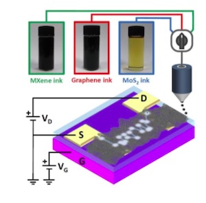
The team investigated three typical types of 2D materials: graphene (a ‘semimetal’ built from a single layer of carbon atoms), molybdenum disulphide (or MoS2, a ‘semiconductor’) and titanium carbide MXene (or Ti3C2, a metal) and mapped how the behaviour of the electrical charge transport changed under these different conditions.
These future devices could one day replace invasive procedures, such as implanting brain electrodes to monitor degenerative conditions that affect the nervous system. Electrodes can only be implanted on a temporary basis, and are uncomfortable for the patient, whereas a flexible device made of biocompatible 2D materials could be integrated with the brain and provide constant monitoring.
Lead researcher Dr Felice Torrisi, from the Department of Chemistry at Imperial, said: “Our results have a huge impact on the way we understand the transport through networks of two-dimensional materials, enabling not only the controlled design and engineering of future printed electronics based on 2D materials, but also new types of flexible electronic devices.
“For example, our work paves the way to reliable wearable devices suitable for biomedical applications, such as the remote monitoring of patients, or bio-implantable devices for long-term monitoring of degenerative diseases or healing processes.”
Other potential healthcare applications include wearable devices for monitoring healthcare – devices like fitness watches, but more integrated with the body, providing sufficiently accurate data to allow doctors to monitor patients without bringing them into hospital for tests.
Optimal designs
The relationships the team discovered between 2D material type and the controls on electrical charge transport will help other researchers design printed and flexible 2D material devices with the properties they desire, based on how they need the electrical charge to act.
They could also reveal how to design entirely new types of electrical components impossible using silicon chips, such as transparent components or ones that modify and transmit light in new ways.
Co-author Professor Renato Gonnelli, from the Politecnico di Torino, Italy, said: “The fundamental understanding of how the electrons are transported through networks of 2D materials underpins the way we manufacture printed electronic components. By identifying the mechanisms responsible for such electronic transport, we will be able to achieve the optimum design of high-performance printed electronics.”
Co-first author Adrees Arbab, from the Department of Chemistry at Imperial and the Cambridge Graphene Centre, said: “In addition, our study could unleash the new electronic and optoelectronic devices exploiting the innovative properties of graphene and other 2D materials, such as incredibly high mobility, optical transparency, and mechanical strength.”
Read the original article, here.
Share on:


Suggested Items
Cadence, TSMC Collaborate on Wide-Ranging Innovations to Transform System and Semiconductor Design
04/25/2024 | Cadence Design SystemsCadence Design Systems, Inc. and TSMC have extended their longstanding collaboration by announcing a broad range of innovative technology advancements to accelerate design, including developments ranging from 3D-IC and advanced process nodes to design IP and photonics.
Ansys, TSMC Enable a Multiphysics Platform for Optics and Photonics, Addressing Needs of AI, HPC Silicon Systems
04/25/2024 | PRNewswireAnsys announced a collaboration with TSMC on multiphysics software for TSMC's Compact Universal Photonic Engines (COUPE). COUPE is a cutting-edge Silicon Photonics (SiPh) integration system and Co-Packaged Optics platform that mitigates coupling loss while significantly accelerating chip-to-chip and machine-to-machine communication.
Siemens’ Breakthrough Veloce CS Transforms Emulation and Prototyping with Three Novel Products
04/24/2024 | Siemens Digital Industries SoftwareSiemens Digital Industries Software launched the Veloce™ CS hardware-assisted verification and validation system. In a first for the EDA (Electronic Design Automation) industry, Veloce CS incorporates hardware emulation, enterprise prototyping and software prototyping and is built on two highly advanced integrated circuits (ICs) – Siemens’ new, purpose-built Crystal accelerator chip for emulation and the AMD Versal™ Premium VP1902 FPGA adaptive SoC (System-on-a-chip) for enterprise and software prototyping.
Elevating PCB Design Engineering With IPC Programs
04/24/2024 | Cory Blaylock, IPCIn a monumental stride for the electronics manufacturing industry, IPC has successfully championed the recognition of the PCB Design Engineer as an official occupation by the U.S. Department of Labor (DOL). This pivotal achievement not only underscores the critical role of PCB design engineers within the technology landscape, but also marks the beginning of a transformative journey toward nurturing a robust, skilled workforce ready to propel our industry into the future.
IPC Design Competition Champion Crowned at IPC APEX EXPO 2024
04/24/2024 | IPCAt IPC APEX EXPO 2024 in Anaheim, California, five competitors squared off to determine who was the best of the best at PCB design.