


 Flexible Thinking: PCB Designers Still Wanted
 Connect the Dots: Five Best Practices for Designing Flex and Rigid-flex PCBs
 Tim’s Takeaways: Human Ingenuity and the Rigid-flex PCB
AT&S Officially Opens New Plant in China
April 22, 2016 | AT&SEstimated reading time: 5 minutes
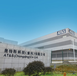
- After Shanghai, another production site opened in China: in the world‘s largest city, Chongqing
- Largest single investment of the AT&S Group, totalling € 480 million; currently 1,700 employees
- Key element in the expansion of technology leadership and further profitable growth of AT&S
- Official opening ceremony with more than 100 guests from politics and business
The site consists of two plants: plant 1 started serial production with one production line in February; plant 2 is currently still being set up. With a total investment volume of roughly € 480 million by 2017, this will be the largest single investment of AT&S to date.
The opening ceremony took place in the presence of representatives of official China and Austria, business, the media, the city of Chongqing, customers, the Supervisory Board and the management of AT&S. The Austrian ambassador in Beijing, Irene Giner-Reichl, Chongqing’s mayor, Huang Qifan, as well as AT&S Supervisory Board Chairman, Hannes Androsch, and CEO Andreas Gerstenmayer held speeches. After the ceremony, selected guests had the opportunity to visit parts of clean room production.
“Chongqing is a key element in the future of AT&S with a view to both technology and positioning, and to further profitable growth. With this plant, we are the first high-end IC substrate manufacturer in China and thus focus on the microelectronics emphasis pursued by the Chinese government at an early stage. Based on the new technologies, combined with the existing high-end technologies, the result is ‘more than AT&S’: we can offer the market new high-end connectivity and advanced packaging solutions and comprehensively position ourselves in the rapidly changing environment of the electronics industry with innovative technologies like IC substrates and wafer level packages for functional modules and the Internet of things. From the PCB top league to the connectivity solution and packaging Champions League, as it were“, says Andreas Gerstenmayer, CEO of AT&S, and adds: “In the medium term, this will entail a new company dimension with revenue of roughly one billion, which will help us to finance future investments from our own cash flow to a greater extent. However, we expect a negative impact during the start-up phase.”
At plant 1, AT&S produces IC substrates, the connection between microchips and printed circuit boards, which are used for microprocessors in computing. Since the start of serial production in late February, the gradual expansion of capacity and the increase in production volume of the complex technology have been proceeding well. From the end of the calendar year 2016, AT&S will gradually start up the second production line for IC substrates. Overall, AT&S will invest roughly € 280 million in property, plant and equipment for this technology by mid-2017.
In addition, the Chongqing site will be extended by a second plant for the latest generation of high-end printed circuit boards, i.e., substrate-like PCBs in order to be able to offer advanced packaging solutions at wafer level. This plant will start production with the first production line in the second half of the calendar year 2016, and with a second production line next year.
Roughly € 200 million will be invested in property, plant and equipment at this plant.
Chen Jian Phua, CEO of the Business Unit Mobile Devices & Substrates, who has been responsible for the establishment of the sites in Shanghai and Chonqing for 12 years for AT&S in leading management positions, outlines the complexity of the technology and the framework conditions: “The new IC substrate technology is not comparable to any technology previously used by AT&S: new, extremely complex production processes in 100 percent cleanroom conditions, new materials as well as a new team, which had to build up know-how in a very short time. We are very proud that we have managed to achieve all this on a very tight schedule. We also invested more than 670,000 hours in training the roughly 1,700 employees who currently work in Chongqing. Sustainable and comprehensive investments in environmental protection have always been important to us at all locations; in Chongqing, about € 24 million have been invested in this area.“
Page 1 of 2
Share on:


Suggested Items
Warm Windows and Streamlined Skin Patches – IDTechEx Explores Flexible and Printed Electronics
04/26/2024 | IDTechExFlexible and printed electronics can be integrated into cars and homes to create modern aesthetics that are beneficial and easy to use. From luminous car controls to food labels that communicate the quality of food, the uses of this technology are endless and can upgrade many areas of everyday life.
iNEMI Packaging Tech Topic Series: Role of EDA in Advanced Semiconductor Packaging
04/26/2024 | iNEMIAdvanced semiconductor packaging with heterogenous integration has made on-package integration of multiple chips a crucial part of finding alternatives to transistor scaling. Historically, EDA tools for front-end and back-end design have evolved separately; however, design complexity and the increased number of die-to-die or die-to-substrate interconnections has led to the need for EDA tools that can support integration of overall design planning, implementation, and system analysis in a single cockpit.
Koh Young Showcases Award-winning Inspection Solutions at SMTconnect with SmartRep in Hall 4A.225
04/25/2024 | Koh Young TechnologyKoh Young Technology, the industry leader in True 3D measurement-based inspection solutions, will showcase an array of award-winning inspection and measurement solutions at SMTconnect alongside its sales partner, SmartRep, in booth 4A.225 at NürnbergMesse from June 11-13, 2023. The following offers a glimpse into what Koh Young will present at the tradeshow:
Real Time with… IPC APEX EXPO 2024: Plasmatreat: Innovative Surface Preparation Solutions
04/25/2024 | Real Time with...IPC APEX EXPOIn this interview, Editor Nolan Johnson speaks with Hardev Grewal, CEO and president of Plasmatreat, a developer of atmospheric plasma solutions. Plasmatreat uses clean compressed air and electricity to create plasma, offering environmentally friendly methods for surface preparation. Their technology measures plasma density for process optimization and can remove organic micro-contamination. Nolan and Hardev also discuss REDOX-Tool, a new technology for removing metal oxides.
Nanotechnology Market to Surpass $53.51 Billion by 2031
04/25/2024 | PRNewswireSkyQuest projects that the nanotechnology market will attain a value of USD 53.51 billion by 2031, with a CAGR of 36.4% over the forecast period (2024-2031).