


 Flexible Thinking: PCB Designers Still Wanted
 Connect the Dots: Five Best Practices for Designing Flex and Rigid-flex PCBs
 Tim’s Takeaways: Human Ingenuity and the Rigid-flex PCB
Fast, Stretchy Circuits Could Yield New Wave of Wearable Electronics
May 30, 2016 | University of Wisconsin-MadisonEstimated reading time: 2 minutes
The consumer marketplace is flooded with a lively assortment of smart wearable electronics that do everything from monitor vital signs, fitness or sun exposure to play music, charge other electronics or even purify the air around you — all wirelessly.
Now, a team of University of Wisconsin—Madison engineers has created the world’s fastest stretchable, wearable integrated circuits, an advance that could drive the Internet of Things and a much more connected, high-speed wireless world.
The advance is a platform for manufacturers seeking to expand the capabilities and applications of wearable electronics — including those with biomedical applications — particularly as they strive to develop devices that take advantage of a new generation of wireless broadband technologies referred to as 5G.With wavelength sizes between a millimeter and a meter, microwave radio frequencies are electromagnetic waves that use frequencies in the .3 gigahertz to 300 gigahertz range. That falls directly in the 5G range.
In mobile communications, the wide microwave radio frequencies of 5G networks will accommodate a growing number of cellphone users and notable increases in data speeds and coverage areas.
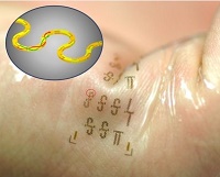
In an intensive care unit, epidermal electronic systems (electronics that adhere to the skin like temporary tattoos) could allow health care staff to monitor patients remotely and wirelessly, increasing patient comfort by decreasing the customary tangle of cables and wires.
What makes the new, stretchable integrated circuits so powerful is their unique structure, inspired by twisted-pair telephone cables. They contain, essentially, two ultra-tiny intertwining power transmission lines in repeating S-curves.
This serpentine shape — formed in two layers with segmented metal blocks, like a 3-D puzzle — gives the transmission lines the ability to stretch without affecting their performance. It also helps shield the lines from outside interference and, at the same time, confine the electromagnetic waves flowing through them, almost completely eliminating current loss. Currently, the researchers’ stretchable integrated circuits can operate at radio frequency levels up to 40 gigahertz.
And, unlike other stretchable transmission lines, whose widths can approach 640 micrometers (or .64 millimeters), the researchers’ new stretchable integrated circuits are just 25 micrometers (or .025 millimeters) thick. That’s tiny enough to be highly effective in epidermal electronic systems, among many other applications.
Ma’s group has been developing what are known as transistor active devices for the past decade. This latest advance marries the researchers’ expertise in both high-frequency and flexible electronics.
“We’ve found a way to integrate high-frequency active transistors into a useful circuit that can be wireless,” says Ma, whose work was supported by the Air Force Office of Scientific Research. “This is a platform. This opens the door to lots of new capabilities.”
Other authors on the paper include Yei Hwan Jung, Juhwan Lee, Namki Cho, Sang June Cho, Huilong Zhang, Subin Lee, Tong June Kim and Shaoqin Gong of UW–Madison and Yijie Qiu of the University of Electronic Science and Technology of China.
Share on:


Suggested Items
Book Excerpt: The Printed Circuit Assembler’s Guide to... Factory Analytics
04/24/2024 | I-Connect007 Editorial TeamIn our fast-changing, deeply competitive, and margin-tight industry, factory analytics can be the key to unlocking untapped improvements to guarantee a thriving business. On top of that, electronics manufacturers are facing a tremendous burden to do more with less. If you don't already have a copy of this book, what follows is an excerpt from the introduction chapter of 'The Printed Circuit Assembler’s Guide to... Factory Analytics: Unlocking Efficiency Through Data Insights' to whet your appetite.
Listen Up! The Intricacies of PCB Drilling Detailed in New Podcast Episode
04/25/2024 | I-Connect007In episode 5 of the podcast series, On the Line With: Designing for Reality, Nolan Johnson and Matt Stevenson continue down the manufacturing process, this time focusing on the post-lamination drilling process for PCBs. Matt and Nolan delve into the intricacies of the PCB drilling process, highlighting the importance of hole quality, drill parameters, and design optimization to ensure smooth manufacturing. The conversation covers topics such as drill bit sizes, aspect ratios, vias, challenges in drilling, and ways to enhance efficiency in the drilling department.
Elevating PCB Design Engineering With IPC Programs
04/24/2024 | Cory Blaylock, IPCIn a monumental stride for the electronics manufacturing industry, IPC has successfully championed the recognition of the PCB Design Engineer as an official occupation by the U.S. Department of Labor (DOL). This pivotal achievement not only underscores the critical role of PCB design engineers within the technology landscape, but also marks the beginning of a transformative journey toward nurturing a robust, skilled workforce ready to propel our industry into the future.
Winner of The Science Show Rakett 69 Receives Incap Scholarship
04/24/2024 | IncapThe winner of the Rakett 69 science show, Andri Türkson, who stood out as an electronics enthusiast, received a scholarship from Incap Estonia, along with an internship opportunity in Saaremaa.
Alternative Manufacturing Inc. Awarded QML Requalification to IPC J-STD-001 and IPC-A-610
04/24/2024 | IPCIPC's Validation Services Program has awarded an IPC J-STD-001 and IPC-A-610 Qualified Manufacturers Listing (QML) requalification to Alternative Manufacturing Inc (AMI).